
We present a technique for direct, in-situ, integration of semiconductor nanowires into photodetectors and other devices. In particular, CdSe nanowire growth off catalyst nanoparticles on metallic electrodes in solution is initiated and controlled by inducing electric fields at the electrode surfaces.
Organization: Massachusetts Institute of Technology
Inventors: August Dorn, Cliff R. Wong, and Moungi G. Bawendi
Primary markets: Semiconductors, Electronics and Chemicals/Materials
Technology Contact: Technology Licensing Office, MIT, US
IP Overview Courtesy of A. Dorn, MIT, US
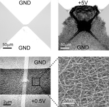
Image: Electrically controlled growth of CdSe nanowires off bismuth catalyst particles attached to platinum electrodes in solution.
Identifying suitable methods for placement and large scale integration of semiconductor nanowires into devices remains one of the major challenges to a wider use of these high potential materials. Our technology overcomes this problem by electrically controlling nanowire growth between electrodes at lithographically predefined sites.
This technique could be of direct interest to the image sensor industry, because it allows for cost-effective and efficient integration of different bandgap semiconductors into photodetector arrays. In addition, nanowires grown off electrodes could find applications in excitonic solar cells, as battery electrodes, in nanoscale transistors, and in sensors where large surface areas are important.
Our technology introduces an inexpensive and practical way to directly integrate a wide variety of semiconductor nanowires into predefined electrode configurations.
Advantages of our approach include low manufacturing costs, high material quality, and low material consumption during the fabrication process. Since we use wet chemistry at moderate temperatures for nanowire growth, no expensive high vacuum equipment is needed for this step. In addition, we are able to electrically induce and limit wire growth to desired sites, so no access precursor material is wasted, as is the case with most conventional fabrication routes. This is particularly important, since many technologically useful semiconductor compounds pose health and environmental risks.
We are looking for industrial partners interested in using our technology to develop new products and fabrication routes. Companies interested in this technology could include Applied Materials, BASF, Bayer, General Electric, Hewlett-Packard, Philips, Siemens and other companies active in the semiconductor and nanotechnology sectors.
